Our research at Dr Choulis Research Group (Molecular Electronics and Photonics Research Unit) is interdisciplinary and multi-faceted. The field of solution-processed electronics is one which requires the expertise and collaboration of chemists, physicists, material scientists and engineers. At the MEP Research Unit our focus is to synthesise, process, characterise and optimise a wide range of solution-processed electronic devices. This page will give you a more detailed overview of our activities.
Material Synthesis and Properties Characterization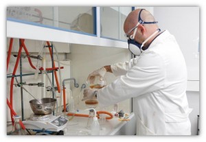
Synthesis of novel materials for solution-processed electronics.Processing of new classes of electronic materials, possessing suitable functionalities for high electronic device performance. Synthesis of buffer layers for long-lived solution-processed electronics.

objectives
- To achieve excellence and breakthrough advances in science and technology by creating an infrastructure capable of taking a leading role in solution processed electronics and photonics.
- To provide a stimulating and challenging environment for the high level training of a new generation of versatile scientists and engineers.
- To contribute to the development of solution-based photovoltaics (Perovskite and Organic PVs) and light emitting diodes (Organic & Perovskite LEDs) technology and other emerging solution-processed electronic devices.
- To contribute to the large scale deployment of low cost printed electronics.
Advanced Characterisation and Morphology
Optical, electrical and morphological characterization studies. Evaluation of material properties relevant to device performance. Device physics studies of novel electronic material systems for advanced applications. Evaluating different approaches for morphological control. Designing electronic material selection rules for optimized solution processed optoelectronic devices.
Electrodes and Interfaces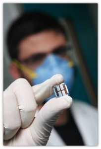

Developing materials and interface engineering methods to provide electrodes with improved carrier selectivity and stability and the necessary experimental and theoretical tools to further improve the basic research knowledge on the physico-chemical interactions and forces at the interfaces of solution-processed PVs and LEDs.
Applying interface engineering concepts in order to improve the stability of anode and cathode interfaces and incorporating new modified buffer layers to solution-processed optoelectronic devices with the aim to achieving optimum performance .
ITO-free and evaporation-free low cost electrodes for printing electronic applications.
Processing of Organic & Perovskite Electronic Devices and Optimisation (Efficiency and Lifetime)
Device optimization of Perovskite and Organic Optoelectronic Devices. Expertise on printing and other solution based processing techniques. Understanding interfaces, development of novel elecrodes and optimizing the processing conditions for maximum device performance (efficiency and lifetime) focusing on materials and procedures needed to be developed for roll-to-roll printing upscaling. Proving that low cost processing capability and improvement in the device performance are directly attributable to the materials/morphology and interface (electrode)/packaging optimization.
Lifetime testing of solution processed optoelectronic devices under real outdoor and accelerated lifetime conditions.
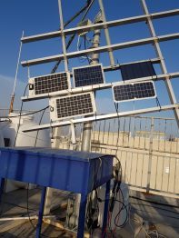 PV Outdoor Testing Unit
Performing characterization and stability tests of large scale solar cells outdoors. Recording of weathering conditions (temperature, irradiation e.t.c.) accompanies the outdoor PV measurements. Data are automatically collected and monitored via wireless transmission methods. The outdoor testing setup is suitable for Monocrystalline, Polycrystalline, CIGS, CdTe, Organic and Hybrid solar cell testing.